David Savastano, Editor03.09.18
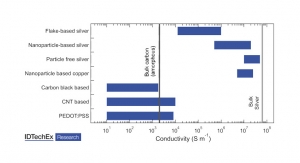
Conductive inks and materials are essential to the world of flexible and printed electronics. It is also a sizable market. IDTechEx has placed the overall value of conductive inks and pastes at $2 billion annually, and in its latest report, “Conductive Ink Markets 2018-2028,” it reports that the market continues to expand.
“The conductive ink industry had a great year last year largely thanks to the record boom year in the photovoltaic industry driven by demand in China,” said Dr. Khasha Ghaffarzadeh, author of the IDTechEx report. “The industry is however still moving ahead with its diversification drive. Here, the industry seeks to find the next big thing, hoping to lessen its overreliance on the photovoltaic industry and other mature industries in which strong competitive pressures persist.
“To this end, the suppliers had been developing as broad a product portfolio as possible seeking to plant their flags in nascent high-potential markets,” Dr. Ghaffarzadeh added.
“This process is now in full swing with several markets transitioning towards commercial fruition this year. The installed base of industrial aerosol machines is expanding, opening the door further to the sales of qualified inks in 3D antenna printing. Printed large-area piezoresistive, capacitive and biosensors are set to become one of the largest constituents of the greater printed electronics industry.” He added that stretchable inks, in-mould electronics (IME) and sprayed on-chip conformal EMI shielding coatings are also strong areas.
Leading conductive ink suppliers note that the flexible and printed electronics market has evolved over the last decade, and they have grown along with the business.
“There is growing interest in adding electronics to everyday items, such as wearables, smart packaging and smart labels,” said Roy Bjorlin, global commercial and strategic initiatives director, Sun Chemical Advanced Materials. “This has created demand to develop materials which provide flexibility and can be processed at high speeds using non-traditional printing methods, such as flexographic printing.”
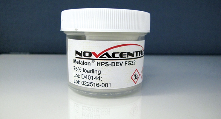
“Over the past 10 years, awareness of the capabilities and value of printed and flexible technologies has really grown in a diversity of industries,” said Stan Farnsworth, VP of marketing at NovaCentrix. “At NovaCentrix we’ve seen a dramatic increase in the number of organizations in the process of implementing printed electronics materials and equipment into their products, with some going all the way into volume production.”
Raghu Das, CEO at IDTechEx, noted that expectations have changed in the last 10 years.
“It’s been typical of many emerging technologies – initially there was hype, mainly involving organizations trying to replace conventional electronics with printed devices, followed by more somber realization of determining uses where printed electronics offers value for the users or product, to where we are today, which is being more clearly focused on key applications, more solution providers and a more mature supply chain, but still with phenomenal innovation occurring at materials, manufacturing and component levels,” Das observed.
“Over the past decade we have really seen the transformation from hype to reality, both in terms of applications coming to market and the materials needed to enable this,” said Kerry Adams, European business development manager, DuPont Advanced Materials. “Results and prototypes delivered by labs and institutes have now crossed over to OEMs and tier 1 suppliers. The hype phase is definitely over.”
“New markets/applications that were pipe dreams 10 years ago, such as wearables, are now realistic,” Alan Brown, applications manager, EMS, Inc., said. “Printed electronics are ideal for this type of application.”
“The market for flexible and printed electronics has increased as more engineers look for ways to make their devices less costly but still reliable,” said Steve Toyama, sales manager at Applied Ink Solutions. “Many of our new clients have commercialized their devices and we expect significant growth coming for these jobs.”
“It has been slower than expected, with both technical and market setbacks, but there is light at the end of the tunnel, with a number of our customers recently launching new products,” said Allen Reid, commercial director at NANOGAP, Inc.
New Opportunities and Materials
Conductive materials suppliers are seeing opportunities as commercialization moves forward. Das said that several markets are poised to be large in the short to medium term – notably in mold electronics and e-textiles.
“We are seeing strong interest in wearables, sensors, in-mold electronics and printed lighting, where our customers have recently launched new products,” Reid said.
“There is a lot of curiosity towards electronic packaging and smart labels, and brand owners are increasingly expressing interest,” Bjorlin said. “The US and European markets appear to be ahead of the curve, and it is likely that production volumes will grow as the traditional packaging converter base starts developing more manufacturing capabilities for electronics at lower costs. For that to happen, the market also needs to determine which functions are to be implemented. This will be largely determined by a combination of cost and benefit analysis as well as consumer acceptance.”
“We’ve seen the adoption in consumer electronics,” said Farnsworth. “Wearables became a flash topic a few years ago and is now settling into a bit more of a maturing stage as companies and consumers determine what is really wanted/needed in product capabilities. We are still in the early stage of the adoption s-curve as companies commit to these technologies in their products.
Sure, some early adopters and market leaders have moved into full-scale implementation, but the majority of the groups we work with are still balancing the investments required in expertise and tooling with market demand.”
“We are seeing an increase in interest in flexible and printed electronics as a means of finding a more cost-effective method of producing functional components and devices for more traditional applications, including sensors/biomarkers and RFID tags,” said Bill Babe, Liquid-X’s sales and marketing manager. “However, flexible and printed electronics also provide the opportunity for more novel applications to be introduced to the market, including organic devices such as thin film PV, OLED lighting and displays. E-textiles are providing new applications for fashion, fitness and health monitoring and many more applications.”
“Wearable applications are constantly of interest, leading to many new exciting applications,” Brown noted.
New advances in materials are helping to drive this growth.
“New material formulations are enabling many new applications from e-textiles to in mold electronics,” Das said.
“The performance targets of silver nanoparticles have been consistent – high conductivity and low temperature sintering, coupled with ink and printing stability,” said Frank Wallace, NANOGAP, Inc.’s technical director. “The requirement for low cost silver nanoparticles has increased in recent years. For silver nanowires, in touch panel applications, there is an increasing requirement for low haze performance and solutions to electro-migration issues. In applications outside of touch panels, the requirement is for good performance (not necessarily low haze) at low cost.”
“Advances in new materials, such as nanomaterials, are going a long way to enhance performance,” Bjorlin said. “Sun Chemical’s pigments development and customized resins also contribute to developing next generation materials with enhanced conductivities as well as adaption to high speed printing, inkjet and aerosol jetting. Printed electronics manufacturers now have the opportunity to process advanced materials at high speeds using non-traditional printing methods that support consumer brands.
“It is clear that printed electronics manufacturers must be convinced that any innovation will enhance the device, be competitive, and have a reliable global supply infrastructure,” Bjorlin added. “This is especially true for smart packaging. For example, nanomaterials such as nanosilver could enable significant advancements in a broad range of applications, including photovoltaic and semiconductor packaging.”
“Customers are now much more educated as far as what their ink requirements are,” said Farnsworth. “Early on in the space, electrical conductivity was the paramount requirement, whereas these days clients know they also need printability and adhesion. We’ve also seen growth in interest in inkjet printing, with clients purchasing systems with integrated print/cure capabilities.”
“The conductive ink industry had a great year last year largely thanks to the record boom year in the photovoltaic industry driven by demand in China,” said Dr. Khasha Ghaffarzadeh, author of the IDTechEx report. “The industry is however still moving ahead with its diversification drive. Here, the industry seeks to find the next big thing, hoping to lessen its overreliance on the photovoltaic industry and other mature industries in which strong competitive pressures persist.
“To this end, the suppliers had been developing as broad a product portfolio as possible seeking to plant their flags in nascent high-potential markets,” Dr. Ghaffarzadeh added.
“This process is now in full swing with several markets transitioning towards commercial fruition this year. The installed base of industrial aerosol machines is expanding, opening the door further to the sales of qualified inks in 3D antenna printing. Printed large-area piezoresistive, capacitive and biosensors are set to become one of the largest constituents of the greater printed electronics industry.” He added that stretchable inks, in-mould electronics (IME) and sprayed on-chip conformal EMI shielding coatings are also strong areas.
Leading conductive ink suppliers note that the flexible and printed electronics market has evolved over the last decade, and they have grown along with the business.
“There is growing interest in adding electronics to everyday items, such as wearables, smart packaging and smart labels,” said Roy Bjorlin, global commercial and strategic initiatives director, Sun Chemical Advanced Materials. “This has created demand to develop materials which provide flexibility and can be processed at high speeds using non-traditional printing methods, such as flexographic printing.”
“Over the past 10 years, awareness of the capabilities and value of printed and flexible technologies has really grown in a diversity of industries,” said Stan Farnsworth, VP of marketing at NovaCentrix. “At NovaCentrix we’ve seen a dramatic increase in the number of organizations in the process of implementing printed electronics materials and equipment into their products, with some going all the way into volume production.”
Raghu Das, CEO at IDTechEx, noted that expectations have changed in the last 10 years.
“It’s been typical of many emerging technologies – initially there was hype, mainly involving organizations trying to replace conventional electronics with printed devices, followed by more somber realization of determining uses where printed electronics offers value for the users or product, to where we are today, which is being more clearly focused on key applications, more solution providers and a more mature supply chain, but still with phenomenal innovation occurring at materials, manufacturing and component levels,” Das observed.
“Over the past decade we have really seen the transformation from hype to reality, both in terms of applications coming to market and the materials needed to enable this,” said Kerry Adams, European business development manager, DuPont Advanced Materials. “Results and prototypes delivered by labs and institutes have now crossed over to OEMs and tier 1 suppliers. The hype phase is definitely over.”
“New markets/applications that were pipe dreams 10 years ago, such as wearables, are now realistic,” Alan Brown, applications manager, EMS, Inc., said. “Printed electronics are ideal for this type of application.”
“The market for flexible and printed electronics has increased as more engineers look for ways to make their devices less costly but still reliable,” said Steve Toyama, sales manager at Applied Ink Solutions. “Many of our new clients have commercialized their devices and we expect significant growth coming for these jobs.”
“It has been slower than expected, with both technical and market setbacks, but there is light at the end of the tunnel, with a number of our customers recently launching new products,” said Allen Reid, commercial director at NANOGAP, Inc.
New Opportunities and Materials
Conductive materials suppliers are seeing opportunities as commercialization moves forward. Das said that several markets are poised to be large in the short to medium term – notably in mold electronics and e-textiles.
“We are seeing strong interest in wearables, sensors, in-mold electronics and printed lighting, where our customers have recently launched new products,” Reid said.
“There is a lot of curiosity towards electronic packaging and smart labels, and brand owners are increasingly expressing interest,” Bjorlin said. “The US and European markets appear to be ahead of the curve, and it is likely that production volumes will grow as the traditional packaging converter base starts developing more manufacturing capabilities for electronics at lower costs. For that to happen, the market also needs to determine which functions are to be implemented. This will be largely determined by a combination of cost and benefit analysis as well as consumer acceptance.”
“We’ve seen the adoption in consumer electronics,” said Farnsworth. “Wearables became a flash topic a few years ago and is now settling into a bit more of a maturing stage as companies and consumers determine what is really wanted/needed in product capabilities. We are still in the early stage of the adoption s-curve as companies commit to these technologies in their products.
Sure, some early adopters and market leaders have moved into full-scale implementation, but the majority of the groups we work with are still balancing the investments required in expertise and tooling with market demand.”
“We are seeing an increase in interest in flexible and printed electronics as a means of finding a more cost-effective method of producing functional components and devices for more traditional applications, including sensors/biomarkers and RFID tags,” said Bill Babe, Liquid-X’s sales and marketing manager. “However, flexible and printed electronics also provide the opportunity for more novel applications to be introduced to the market, including organic devices such as thin film PV, OLED lighting and displays. E-textiles are providing new applications for fashion, fitness and health monitoring and many more applications.”
“Wearable applications are constantly of interest, leading to many new exciting applications,” Brown noted.
New advances in materials are helping to drive this growth.
“New material formulations are enabling many new applications from e-textiles to in mold electronics,” Das said.
“The performance targets of silver nanoparticles have been consistent – high conductivity and low temperature sintering, coupled with ink and printing stability,” said Frank Wallace, NANOGAP, Inc.’s technical director. “The requirement for low cost silver nanoparticles has increased in recent years. For silver nanowires, in touch panel applications, there is an increasing requirement for low haze performance and solutions to electro-migration issues. In applications outside of touch panels, the requirement is for good performance (not necessarily low haze) at low cost.”
“Advances in new materials, such as nanomaterials, are going a long way to enhance performance,” Bjorlin said. “Sun Chemical’s pigments development and customized resins also contribute to developing next generation materials with enhanced conductivities as well as adaption to high speed printing, inkjet and aerosol jetting. Printed electronics manufacturers now have the opportunity to process advanced materials at high speeds using non-traditional printing methods that support consumer brands.
“It is clear that printed electronics manufacturers must be convinced that any innovation will enhance the device, be competitive, and have a reliable global supply infrastructure,” Bjorlin added. “This is especially true for smart packaging. For example, nanomaterials such as nanosilver could enable significant advancements in a broad range of applications, including photovoltaic and semiconductor packaging.”
“Customers are now much more educated as far as what their ink requirements are,” said Farnsworth. “Early on in the space, electrical conductivity was the paramount requirement, whereas these days clients know they also need printability and adhesion. We’ve also seen growth in interest in inkjet printing, with clients purchasing systems with integrated print/cure capabilities.”