David Savastano, Editor11.07.14
There have been plenty of interesting printed electronics systems that have been designed in recent years. However, having a good idea usually isn’t enough to guarantee success. Simply put, if the product can’t actually be manufactured at a reasonable cost, the new application will never see the light of day.
The ability to bring a product from the lab to fab is a critical step in its future success. To that end, some successful printers have decided that the printed electronics market is a good field to bring their years of experience.
Si-Cal, Inc., a heat transfer label and printed electronics specialist, found that the printed electronics field was ideal for its high quality capabilities and entered the field in 2005, when the company began screenprinting RFID antennas.
“We saw printed electronics as a way to diversify what we do,” said Jaye Tyler, president of Si-Cal. “While we continued to grow our Graphics Division, we also knew we could leverage our existing equipment into printed electronics, and a lot of the skill set in printing layers of graphics translates well into electronics.”
GSI Technologies, LLC has been manufacturing printed electronics systems for more than 15 years. Dr. Gordon Smith, chief technology officer at GSI Technologies, said that technical expertise is key to success with printing these systems.
“It is a high growth, technology driven market where you can differentiate based on your technical expertise,” Dr. Smith said.
Jason Herndon, Instant INTAQ manager at GM Nameplate, said that GM Nameplate entered the PE market as a screenprinted membrane switch manufacturer more than 20 years ago.
“Our company has been focused on printed labels, nameplates, overlays and similar products for the aerospace, medical and consumer electronics industries for nearly 60 years,” Herndon said. “The transition into screenprinted electronics was a logical next step in serving the needs of our customers.”
Wolfgang Mildner, managing director for PolyIC GmbH & Co. KG, said that PolyIC have been in the PE market from the very beginning of the foundation of PolyIC as a joint venture between Leonhard Kurz Stiftung & Co. KG and Siemens AG (Kurz now fully owns PolyIC).
“PolyIC is called the ‘Chip Printers,’ which already tells our vision from its name,” Mildner added.
Tom Hartmann, medical director BP/Electronics at Topflight, said that Topflight started out in 1943 as a precision machine shop, and began building its own advanced presses which quickly progressed to printing pressure sensitive labels in the 1950s.
“Throughout the 1960s, it increasingly rose up to take on greater challenges, shrink films and self destruct labels among them,” Hartmann added. “In the 1970s, a very different kind of challenge came up, labels or printed materials that did something, a function, that being conducting electric current. It was no longer just a printer of exotic materials and inks working with ever increasing complexity and capabilities, but a new type of ‘flex circuit’ company manufacturing membrane switches and sensors.
“But why did we do it?” Hartmann asked. “Our customers. They were the ones that drove Topflight, by requesting further capabilities in what printed conductives could do at the time and pushing our people into further modifying equipment, using novel conductive polymer thick films and effectively printing on stabilized materials for circuits. This allowed it to reach out further into new processes as well and to search the globe for even more conductive ink-receptive substrates to satisfy their needs. This ever-increase tool set opened it up to help many others as well.
“What also allowed this was Topflight’s ability to work off a solid platform in graphic printing with various print methods already in play and multiple substrates with specialized ink systems running daily,” Hartmann concluded. “This encouraged Topflight to branch out into many types of printed conductives. We added a technical staff to support this effort, which became the catalyst to dive into new and evolving technologies. Most printing companies do not carry an R&D department to develop their processes for the future, especially at this time in printed conductives. We have a growing foothold in medical applications, which constantly seek value added steps from their suppliers and more functionality in their products, which biosensors provide, for example. Early creativity in RFID applications provided the impetus to acquire the necessary equipment to enhance our portfolio of capabilities.”
There are a wide variety of printing and roll-to-roll processes used in printed electronics. Screenprinting is the most frequent choice; Si-Cal, for example, only uses roll-to-roll screenprinting. Other manufacturers are working on flexo, gravure and inkjet.
Dr. Smith noted that GSI Technologies uses primarily screenprinting, either sheet or roll-to-roll, while Herndon said that GM Nameplate primarily focuses on screenprinting, but also has lithographic, flexographic and digital printing capabilities.
Hartmann noted that Topflight currently utilizes screen and flexography for printed electronics, but in the past, it has used gravure to print such things as glucose test strips as well as EKG electrodes.
“Modules required to expand press capabilities and the higher tooling economics for gravure moved screen and flexo along in printed electronics as more feasible choices to achieve customer ROI,” Hartmann said. “An added discovery was that Topflight found its growing capabilities with screen and flexo also covered the gamut of what it required to satisfy the needs of the printed electronics world.
“However, printing by itself isn’t enough,” Hartmann added. “The complement of newer converting capabilities allowed it to more fully complete product requirements. Things such as servo motors to re-register to our own printed webs, or others provided by our customers, allowed it to add multiple layers to a single component. In many cases, these components required printed graphics or other functional inks/coatings for protection or add indicators such as thermochromics, dielectrics and the like, as well as layered conductive and non-conductive printing.”
“We have tried and used several nearly all standard printing processes, except maybe inkjet,” Mildner said. “We have even developed a new proprietary R2R process, which allows us to go beyond current limitations.”
Current Products on the Market
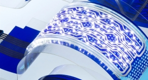
There is a wide range of products being printed today, ranging from medical patches and sensors to RFID and much more.
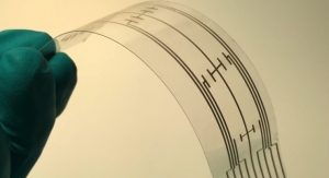
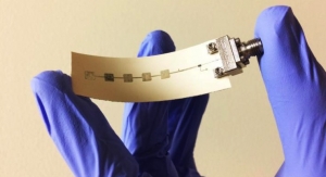
Hartmann noted that Topflight has printed many different products, including early printed transistors, electronic memory converting, various printed antennae, glucose sensor components, trial work for solar panels using nano silver and printed grapheme security devices as well as aluminum security device components.
Hartmann added that the early printed transistors were screenprinted, followed by a dielectric layer and a subsequent conductive layer, and the base layers were done in conductive silver and silver/carbon blends, aluminum and copper. The printed antennae were done screen as well as flexo, primarily with conductive silver. Topflight also prints dry resist followed by chemical etch of alum and copper as well as a seed layer of silver followed by plate up of copper. For RFID, Topflight doesn’t attach the chip, but will come back and finish the final conversion after it prints the antenna, including system testing. The glucose sensors components are printed by gravure and flexo, and consist of carbon as well as screened carbon/silver blend. The trial work for solar panels uses nano silver, requiring narrow line flexo work with line widths down to 35 microns that were continuous and conductive.
Dr. Smith noted that GSI Technologies has printed a wide range of products, with electroluminescent lamps and medical diagnostic test strips being two successful examples. Tyler said that Si-Cal has successfully produced iontophoretic patches, sensors, displays, EKG devices, wearable nerve stimulation and sensing systems and more complex RFID for security and anti-counterfeiting, while Herndon noted that GM Nameplate has printed membrane switches, medical electrodes, capacitive and force sensors and iontophoresis patches. Mildner said that PolyIC’s main product today is PolyTC, a transparent conductive film PolyIC is using for touch sensors and EMI applications.
Overcoming Challenges
Having the right equipment and knowledge and experience in printing is obviously a good start in producing printed electronics. However, there are other hurdles that have to be overcome. Hartmann said that there are two broad challenges: technical capabilities and customer requirements.
“If our customer isn’t quite clear as to the ultimate goal or has become too locked into a product, then the odds of commercialization become smaller,” Hartmann said. “We’ve had customers who are dead set on a particular resistance goal with tight tolerances and a trace design that on paper should work. This can block us from using the best techniques and our creativity to create circuit designs to get to the same end result. Education from both sides is key here. One Topflight marking entry called ‘Space Saver’ showed how we can get the same performance in a smaller footprint by changing the trace size or conductive ink (PTF versus nano).
“Some customers want very small feature sizes but high end material performance,” Hartmann added. “For example, a solid block of printed silver yields different conductivity results than the same ink being printed in a 3-mil line and space. Matching the right tooling (plates, aniloxes, screens and dies) to the print process along with the inks and substrates are all part of the considerations and challenges. Each combination yields slightly different results when put together, such as ink wet out or mesh count, and all variables must be dialed in through press trials. We forego the aggravation of scale up from lab to press floor since we can do trials with our production equipment. We get requests that run the gamut of feature size, performance and materials.”
Herndon said that scaling up to production and quality control and inspection are two key areas for printers.
“As the feature sizes of printed electronics are reduced, the greatest challenges are scaling to high volume production and developing the appropriate quality control metrics and supporting inspection tools,” Herndon said. “Our engineering team has designed a number of custom tools to help overcome these challenges.
“I believe that the market will continue to push for smaller feature sizes, tighter registration tolerances, lower cost materials and greater throughput,” Herndon added.
“There are very demanding manufacturing requirements which we have been able to meet,” Tyler said. “These systems are multi-layer and have very tight tolerances. The time to production is also very challenging because it is so long, and there can be a lot of steps to go through before the product gets to market.”
Mildner said that partnerships are key to solving these challenges.
“There are huge challenges still to overcome or under development that will not to be solved by a single company,” Mildner observed. “Collaboration is needed. For example, to produce circuits and chips, good materials are needed, semiconductors with good performance (mobility on/off ratio) or new classes of materials scaled up for mass production (n-type semiconductors).
Another challenge is functional quality control of a roll-to-roll production process to achieve and control reasonable yield.”
The Future of the Printed Electronics Market
One way to tell if the printed electronics market is growing is by talking with printers and converters, and the industry leaders I spoke with say that they are seeing more business coming their way.
“Definitely interest has been growing,” Dr. Smith noted. “At GSI, we are focused on medical, automotive, and consumer electronic applications. Product solutions will encompass supplying components as well as fully integrated devices.”
“We see interest growing,” Tyler said. “We have a very deep pipeline of opportunities.”
Mildner said that PolyIC is currently seeing more demand in sensors and enhancing surfaces to be functional, such as for touch functions.
“This demand is coming from various markets: mobile phones, automotive, consumer electronics and white goods,” Mildner said. “All of them want either displays with touch functions or want to replace mechanical keys by touch key functions. In the future, more intelligence or even lighting functions will be integrated in the human interface. There is a lot of potential for printed electronics, but also the intelligence of packaging and products will be enhanced by identification, intelligence and sensors, bringing us back to the original vision of PolyIC.”
“We have an ever-increasing foothold in medical PE applications, which constantly seek value added steps from their suppliers and more functionality in their products, including such things as printed biosensors, lateral flow test strips with printed circuits and many others,” Hartmann concluded. “RFID applications have advanced with multi-sensing, and low cost printed touch sensors are starting to move into many different areas.”
The ability to bring a product from the lab to fab is a critical step in its future success. To that end, some successful printers have decided that the printed electronics market is a good field to bring their years of experience.
Si-Cal, Inc., a heat transfer label and printed electronics specialist, found that the printed electronics field was ideal for its high quality capabilities and entered the field in 2005, when the company began screenprinting RFID antennas.
“We saw printed electronics as a way to diversify what we do,” said Jaye Tyler, president of Si-Cal. “While we continued to grow our Graphics Division, we also knew we could leverage our existing equipment into printed electronics, and a lot of the skill set in printing layers of graphics translates well into electronics.”
GSI Technologies, LLC has been manufacturing printed electronics systems for more than 15 years. Dr. Gordon Smith, chief technology officer at GSI Technologies, said that technical expertise is key to success with printing these systems.
“It is a high growth, technology driven market where you can differentiate based on your technical expertise,” Dr. Smith said.
Jason Herndon, Instant INTAQ manager at GM Nameplate, said that GM Nameplate entered the PE market as a screenprinted membrane switch manufacturer more than 20 years ago.
“Our company has been focused on printed labels, nameplates, overlays and similar products for the aerospace, medical and consumer electronics industries for nearly 60 years,” Herndon said. “The transition into screenprinted electronics was a logical next step in serving the needs of our customers.”
Wolfgang Mildner, managing director for PolyIC GmbH & Co. KG, said that PolyIC have been in the PE market from the very beginning of the foundation of PolyIC as a joint venture between Leonhard Kurz Stiftung & Co. KG and Siemens AG (Kurz now fully owns PolyIC).
“PolyIC is called the ‘Chip Printers,’ which already tells our vision from its name,” Mildner added.
Tom Hartmann, medical director BP/Electronics at Topflight, said that Topflight started out in 1943 as a precision machine shop, and began building its own advanced presses which quickly progressed to printing pressure sensitive labels in the 1950s.
“Throughout the 1960s, it increasingly rose up to take on greater challenges, shrink films and self destruct labels among them,” Hartmann added. “In the 1970s, a very different kind of challenge came up, labels or printed materials that did something, a function, that being conducting electric current. It was no longer just a printer of exotic materials and inks working with ever increasing complexity and capabilities, but a new type of ‘flex circuit’ company manufacturing membrane switches and sensors.
“But why did we do it?” Hartmann asked. “Our customers. They were the ones that drove Topflight, by requesting further capabilities in what printed conductives could do at the time and pushing our people into further modifying equipment, using novel conductive polymer thick films and effectively printing on stabilized materials for circuits. This allowed it to reach out further into new processes as well and to search the globe for even more conductive ink-receptive substrates to satisfy their needs. This ever-increase tool set opened it up to help many others as well.
“What also allowed this was Topflight’s ability to work off a solid platform in graphic printing with various print methods already in play and multiple substrates with specialized ink systems running daily,” Hartmann concluded. “This encouraged Topflight to branch out into many types of printed conductives. We added a technical staff to support this effort, which became the catalyst to dive into new and evolving technologies. Most printing companies do not carry an R&D department to develop their processes for the future, especially at this time in printed conductives. We have a growing foothold in medical applications, which constantly seek value added steps from their suppliers and more functionality in their products, which biosensors provide, for example. Early creativity in RFID applications provided the impetus to acquire the necessary equipment to enhance our portfolio of capabilities.”
There are a wide variety of printing and roll-to-roll processes used in printed electronics. Screenprinting is the most frequent choice; Si-Cal, for example, only uses roll-to-roll screenprinting. Other manufacturers are working on flexo, gravure and inkjet.
Dr. Smith noted that GSI Technologies uses primarily screenprinting, either sheet or roll-to-roll, while Herndon said that GM Nameplate primarily focuses on screenprinting, but also has lithographic, flexographic and digital printing capabilities.
Hartmann noted that Topflight currently utilizes screen and flexography for printed electronics, but in the past, it has used gravure to print such things as glucose test strips as well as EKG electrodes.
“Modules required to expand press capabilities and the higher tooling economics for gravure moved screen and flexo along in printed electronics as more feasible choices to achieve customer ROI,” Hartmann said. “An added discovery was that Topflight found its growing capabilities with screen and flexo also covered the gamut of what it required to satisfy the needs of the printed electronics world.
“However, printing by itself isn’t enough,” Hartmann added. “The complement of newer converting capabilities allowed it to more fully complete product requirements. Things such as servo motors to re-register to our own printed webs, or others provided by our customers, allowed it to add multiple layers to a single component. In many cases, these components required printed graphics or other functional inks/coatings for protection or add indicators such as thermochromics, dielectrics and the like, as well as layered conductive and non-conductive printing.”
“We have tried and used several nearly all standard printing processes, except maybe inkjet,” Mildner said. “We have even developed a new proprietary R2R process, which allows us to go beyond current limitations.”
Current Products on the Market
There is a wide range of products being printed today, ranging from medical patches and sensors to RFID and much more.
Hartmann noted that Topflight has printed many different products, including early printed transistors, electronic memory converting, various printed antennae, glucose sensor components, trial work for solar panels using nano silver and printed grapheme security devices as well as aluminum security device components.
Hartmann added that the early printed transistors were screenprinted, followed by a dielectric layer and a subsequent conductive layer, and the base layers were done in conductive silver and silver/carbon blends, aluminum and copper. The printed antennae were done screen as well as flexo, primarily with conductive silver. Topflight also prints dry resist followed by chemical etch of alum and copper as well as a seed layer of silver followed by plate up of copper. For RFID, Topflight doesn’t attach the chip, but will come back and finish the final conversion after it prints the antenna, including system testing. The glucose sensors components are printed by gravure and flexo, and consist of carbon as well as screened carbon/silver blend. The trial work for solar panels uses nano silver, requiring narrow line flexo work with line widths down to 35 microns that were continuous and conductive.
Dr. Smith noted that GSI Technologies has printed a wide range of products, with electroluminescent lamps and medical diagnostic test strips being two successful examples. Tyler said that Si-Cal has successfully produced iontophoretic patches, sensors, displays, EKG devices, wearable nerve stimulation and sensing systems and more complex RFID for security and anti-counterfeiting, while Herndon noted that GM Nameplate has printed membrane switches, medical electrodes, capacitive and force sensors and iontophoresis patches. Mildner said that PolyIC’s main product today is PolyTC, a transparent conductive film PolyIC is using for touch sensors and EMI applications.
Overcoming Challenges
Having the right equipment and knowledge and experience in printing is obviously a good start in producing printed electronics. However, there are other hurdles that have to be overcome. Hartmann said that there are two broad challenges: technical capabilities and customer requirements.
“If our customer isn’t quite clear as to the ultimate goal or has become too locked into a product, then the odds of commercialization become smaller,” Hartmann said. “We’ve had customers who are dead set on a particular resistance goal with tight tolerances and a trace design that on paper should work. This can block us from using the best techniques and our creativity to create circuit designs to get to the same end result. Education from both sides is key here. One Topflight marking entry called ‘Space Saver’ showed how we can get the same performance in a smaller footprint by changing the trace size or conductive ink (PTF versus nano).
“Some customers want very small feature sizes but high end material performance,” Hartmann added. “For example, a solid block of printed silver yields different conductivity results than the same ink being printed in a 3-mil line and space. Matching the right tooling (plates, aniloxes, screens and dies) to the print process along with the inks and substrates are all part of the considerations and challenges. Each combination yields slightly different results when put together, such as ink wet out or mesh count, and all variables must be dialed in through press trials. We forego the aggravation of scale up from lab to press floor since we can do trials with our production equipment. We get requests that run the gamut of feature size, performance and materials.”
Herndon said that scaling up to production and quality control and inspection are two key areas for printers.
“As the feature sizes of printed electronics are reduced, the greatest challenges are scaling to high volume production and developing the appropriate quality control metrics and supporting inspection tools,” Herndon said. “Our engineering team has designed a number of custom tools to help overcome these challenges.
“I believe that the market will continue to push for smaller feature sizes, tighter registration tolerances, lower cost materials and greater throughput,” Herndon added.
“There are very demanding manufacturing requirements which we have been able to meet,” Tyler said. “These systems are multi-layer and have very tight tolerances. The time to production is also very challenging because it is so long, and there can be a lot of steps to go through before the product gets to market.”
Mildner said that partnerships are key to solving these challenges.
“There are huge challenges still to overcome or under development that will not to be solved by a single company,” Mildner observed. “Collaboration is needed. For example, to produce circuits and chips, good materials are needed, semiconductors with good performance (mobility on/off ratio) or new classes of materials scaled up for mass production (n-type semiconductors).
Another challenge is functional quality control of a roll-to-roll production process to achieve and control reasonable yield.”
The Future of the Printed Electronics Market
One way to tell if the printed electronics market is growing is by talking with printers and converters, and the industry leaders I spoke with say that they are seeing more business coming their way.
“Definitely interest has been growing,” Dr. Smith noted. “At GSI, we are focused on medical, automotive, and consumer electronic applications. Product solutions will encompass supplying components as well as fully integrated devices.”
“We see interest growing,” Tyler said. “We have a very deep pipeline of opportunities.”
Mildner said that PolyIC is currently seeing more demand in sensors and enhancing surfaces to be functional, such as for touch functions.
“This demand is coming from various markets: mobile phones, automotive, consumer electronics and white goods,” Mildner said. “All of them want either displays with touch functions or want to replace mechanical keys by touch key functions. In the future, more intelligence or even lighting functions will be integrated in the human interface. There is a lot of potential for printed electronics, but also the intelligence of packaging and products will be enhanced by identification, intelligence and sensors, bringing us back to the original vision of PolyIC.”
“We have an ever-increasing foothold in medical PE applications, which constantly seek value added steps from their suppliers and more functionality in their products, including such things as printed biosensors, lateral flow test strips with printed circuits and many others,” Hartmann concluded. “RFID applications have advanced with multi-sensing, and low cost printed touch sensors are starting to move into many different areas.”