David Savastano, Editor03.22.17
As flexible and printed electronics find new commercial markets, manufacturers are seeking improved performance from conductive inks and other materials. As a result, suppliers are developing new materials for their customers.
Sarah Wilson, product promotion specialist II at Brewer Science, Inc., noted that the requirement of conductive inks can be divided into two categories based on their use. First, there are transparent conductive inks for applications such as replacement of indium tin oxide, photonic and optical devices, display, solar cells, and touchscreens. Second, there are conductive inks for interconnects in flexible printed electronic devices such as transistors and oscillators.
“We produce semiconducting CNTs inks for multiple printing tools such as ink jet, screen, and Aerosol Jet, giving competitive edges to our sensor products,” Wilson said. “Our requirements mostly encompass a response to a given stimulus. Brewer Science has enabled advancement of diverse technologies in various industries such as semiconductor, electronics packaging, and printed electronics. The program has a structured joint development program to effectively launch mutually beneficial and high-value collaborations with domestic and global government organizations, academic institutions, consortia, and commercial entities.”
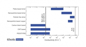
Dr. Allen Reid, commercial director for NANOGAP, said that manufacturers are looking for thinner diameters for silver nanowires.
“For silver nanowires, our customers are asking for thinner diameter in order to improve optical properties and efficiency (lower silver usage levels),” said Dr. Reid. “For silver nanoparticles our customers are asking for improved conductivity and low temperature sintering properties.”
Stan Farnsworth, VP of marketing for NovaCentrix, pointed out that cost, performance and service are important to customers.
“From an ability to deliver successful conductive products to the manufacturers, we are of course asked to deliver products as implementable price points, and with great performance such as with electrical conductivity, strong adhesion to substrates, and reliable printability,” Farnsworth noted. “What NovaCentrix also provides, though, is the benefit of the world-class expertise of our technical team. We routinely work with our clients to solve system-level technology integration and performance problems in their product development process. Our down-stream adopters are relying on us to help their products launch on-time and on-budget, which we are able to do because of our expertise in materials, printing and processing.”
“Manufacturers most often are looking for competitive pricing and high throughput production together with high quality and performance,” Fernando de la Vega, CEO of PV Nano Cell, said.
Kerry Adams, printed electronics market segment manager, DuPont, said that performance demands for conductive inks and pastes are increasing all the time.
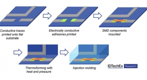
“Apart from the obvious requirements of conductivity, fine line resolution, adhesion and flexibility, the new applications require stretchability, washability and formability,” Adams reported. “The ability to supply materials that are digitally printed is becoming important, as is the need for complete systems of materials and substrates to function effectively together in complex multilayer builds. Finally, we are also seeing demand to take printed electronics inks to both lower and higher temperatures, allowing an expanded range of substrate types and applications.”
“The primary requirements are stretchability, washability and high abrasion resistance,” Matt Ganslaw, VP, sales for Creative Materials, added. “Another major demand from our customers in the wearables industry is to effectively make electrical attachment of circuitry and sensors using flexible conductive adhesives.”
“The obvious answer is more conductivity and lower price, but the more difficult problem is the UV dielectric,” said Steve Toyama of Applied Ink Solutions. “Typically, a customer is looking for high flexibility with a good moisture resistance to help prevent silver migration in the crossover.”
Dr. Daniel Harrison, SVP R&D at IIMAK, said that customers demand low resistance, sharp continuous traces and no post printing treatments (i.e. sintering), adding that metallograph offers a unique digital print solution that can deliver these required attributes.
“It is clear that printed electronics manufacturers must be convinced that any innovation will enhance the device, be competitive, and have a reliable global supply infrastructure,” concluded Roy Bjorlin, global commercial and strategic initiatives director, Sun Chemical Advanced Materials. “This is especially true for smart packaging. For example, nanomaterials such as nanosilver could enable significant advancements in a broad range of applications, including photovoltaic and semiconductor packaging.”
Sarah Wilson, product promotion specialist II at Brewer Science, Inc., noted that the requirement of conductive inks can be divided into two categories based on their use. First, there are transparent conductive inks for applications such as replacement of indium tin oxide, photonic and optical devices, display, solar cells, and touchscreens. Second, there are conductive inks for interconnects in flexible printed electronic devices such as transistors and oscillators.
“We produce semiconducting CNTs inks for multiple printing tools such as ink jet, screen, and Aerosol Jet, giving competitive edges to our sensor products,” Wilson said. “Our requirements mostly encompass a response to a given stimulus. Brewer Science has enabled advancement of diverse technologies in various industries such as semiconductor, electronics packaging, and printed electronics. The program has a structured joint development program to effectively launch mutually beneficial and high-value collaborations with domestic and global government organizations, academic institutions, consortia, and commercial entities.”
Dr. Allen Reid, commercial director for NANOGAP, said that manufacturers are looking for thinner diameters for silver nanowires.
“For silver nanowires, our customers are asking for thinner diameter in order to improve optical properties and efficiency (lower silver usage levels),” said Dr. Reid. “For silver nanoparticles our customers are asking for improved conductivity and low temperature sintering properties.”
Stan Farnsworth, VP of marketing for NovaCentrix, pointed out that cost, performance and service are important to customers.
“From an ability to deliver successful conductive products to the manufacturers, we are of course asked to deliver products as implementable price points, and with great performance such as with electrical conductivity, strong adhesion to substrates, and reliable printability,” Farnsworth noted. “What NovaCentrix also provides, though, is the benefit of the world-class expertise of our technical team. We routinely work with our clients to solve system-level technology integration and performance problems in their product development process. Our down-stream adopters are relying on us to help their products launch on-time and on-budget, which we are able to do because of our expertise in materials, printing and processing.”
“Manufacturers most often are looking for competitive pricing and high throughput production together with high quality and performance,” Fernando de la Vega, CEO of PV Nano Cell, said.
Kerry Adams, printed electronics market segment manager, DuPont, said that performance demands for conductive inks and pastes are increasing all the time.
“Apart from the obvious requirements of conductivity, fine line resolution, adhesion and flexibility, the new applications require stretchability, washability and formability,” Adams reported. “The ability to supply materials that are digitally printed is becoming important, as is the need for complete systems of materials and substrates to function effectively together in complex multilayer builds. Finally, we are also seeing demand to take printed electronics inks to both lower and higher temperatures, allowing an expanded range of substrate types and applications.”
“The primary requirements are stretchability, washability and high abrasion resistance,” Matt Ganslaw, VP, sales for Creative Materials, added. “Another major demand from our customers in the wearables industry is to effectively make electrical attachment of circuitry and sensors using flexible conductive adhesives.”
“The obvious answer is more conductivity and lower price, but the more difficult problem is the UV dielectric,” said Steve Toyama of Applied Ink Solutions. “Typically, a customer is looking for high flexibility with a good moisture resistance to help prevent silver migration in the crossover.”
Dr. Daniel Harrison, SVP R&D at IIMAK, said that customers demand low resistance, sharp continuous traces and no post printing treatments (i.e. sintering), adding that metallograph offers a unique digital print solution that can deliver these required attributes.
“It is clear that printed electronics manufacturers must be convinced that any innovation will enhance the device, be competitive, and have a reliable global supply infrastructure,” concluded Roy Bjorlin, global commercial and strategic initiatives director, Sun Chemical Advanced Materials. “This is especially true for smart packaging. For example, nanomaterials such as nanosilver could enable significant advancements in a broad range of applications, including photovoltaic and semiconductor packaging.”