David Savastano, Editor12.02.15
Conductive inks are a critical component in printed electronics, with unique properties required for inkjet and other printing processes. With interest growing in 3D printing of conductive materials, conductive ink manufacturers are developing new products for this market.
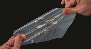
PV Nano Cell (PVN) is one company that is making gains in 3D printing. Founded in 2009, PVN was initially focused on the photovoltaic (PV) market, developing its Sicrys portfolio of single-crystal nanometric conductive nano silver and copper inks for inkjet printing on flexible substrates. PVN has since branched out into a wide range of end uses, including sensors, RFID, touchscreens and printed circuit boards.
Most recently, PV Nano Cell has moved into the 3D printing space, working with a major 3D printer manufacturer on developing conductive inks. This led to the company receiving the award for Best Development in Materials for 3D Printing from IDTechEx during Printed Electronics USA 2015 in November 2015.
“We created PVN as we strongly believed that additive manufacturing must be implemented in the production of electronic devices, not only to lower costs, expand capabilities (3D printing) but also to reduce the amount of hazardous wastes and make our world ‘cleaner’ and sustainable,” said Dr. Fernando de la Vega, CEO of PV Nano Cell. “The perfect fit for additive manufacturing in the electronic production field is inkjet digital printing, and to make inkjet metal conductive inks, nano metal particles are a must, the only viable solution.
“PVN has been created on the basis of a very innovative, out of the box thinking technology to make nano metal particles,” Dr. de la Vega added. “Our Sicrys family of inks is produced via a clean very efficient production process which doesn’t produce hazardous wastes. The nano-metric particles that are the result of our process are the most suitable to formulate commercial viable inks for mass production applications.”
The company has created inks for a variety of markets. “We are currently targeting photovoltaics, antennas for mobile phones, antennas for Internet of Things (IoT) devices, printed circuit boards (PCBs), sensors, security and flexible and customized electronics, as well as 2.5D and 3D printed electronics,” said Dr. de la Vega.
Dr. de la Vega said that the largest challenge that PV Nano Cell has had to overcome has been the lack of mass market applications and production tools, including printers.
“Our Sicrys inks were manufactured for large-scale printing applications,” he said. “Many of our potential customers are not using a printed electronics solution but stand to benefit greatly by adopting it for large-scale printing applications. To try and ease the adoption of our Sicrys technology, we have developed our ‘complete solution’ offer. We provide the printer needed in order to keep the customer from having to shop for one that is suitable for digital inkjet printing. When they come to us, they receive everything they need to begin the transition.”
Dr. de la Vega noted that inkjet printing offers a range of benefits.
“Since the printing is non-touch, there is no significant impact on the substrate, and as the inks can be sintered at low temperatures, they enable printing on flexible, temperature-sensitive substrates made of plastic, fabric or even paper, as well as 3D printed electronics,” he said.
Inkjet printing can also reduce the overall amount of hazardous waste generated in the production of electronic devices and lower production costs, enabling low-cost electronics in different applications, including flexible electronics and sensors. It can also enable the digital printing of customized and 3D electronics.
Dr. de la Vega sees plenty of opportunities for printed and flexible electronics.
“Printed and flexible electronics have come a long way in a short time,” he noted. “However, in order for the industry to experience true growth and success, it requires cost-effective, competitively priced digital conductive inks and equipment and processes suitable for industrial mass production.
'PV Nano Cell is bringing the solutions to these gaps in the market,” he added. “With the industry’s adoption of the right technologies, we anticipate additional applications and enhanced capabilities for digital printing, for example, even narrower patterns, which means gaining greater efficiency with less material and lower costs; additional inks with different metals and functionalities; and inkjet printing of embedded passive components in PCBs, followed closely by 3D and customized printed electronics. Digital printing will revolutionize the industry by lowering costs as well as adding significantly increased design flexibility.”