David Savastano, Editor10.28.15
The worlds of printed electronics and 3D printing are both drawing a lot of interest, but interestingly, there is very little intersection between the two technologies. Nano Dimension is in a good position to change that.
Founded in 2012, Nano Dimension is an Israel-based startup with a range of expertise, developing its own 3D printers, conductive inkjet inks and software. The company has grown to the point where it is now listed on the Tel Aviv Stock Exchange.
“Our mission is to bring together printed electronics and 3D printing,” said Simon Fried, chief marketing officer for Nano Dimension. “We are developing a 3D printer for printed circuit boards (PCBs), as well as our own conductive silver nanoparticle inks and inkjettable dielectric inks. We believe we are one of the few companies that make the ink, software and printers.
“The 3D printed electronics space is a new area, and there are not many companies in this space,” Fried added. “There has not been very much overlap with printed electronics.”
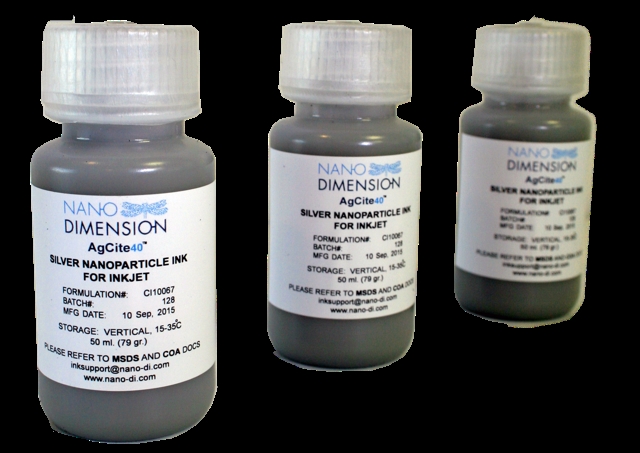
Nano Dimension just launched its AgCiteTMline of conductive silver nanoparticle inks for inkjet deposition. Fried noted that AgCite inks offer exceptionally reliable printability and excellent electrical properties, and sinters at low temperatures. This allows the inks to be printed on a broad range of substrates, including paper, films, glass, metals and coatings.
A portion of Nano Dimension’s nanoparticle synthesis technology for its new AgCite inkjet inks is licensed through Prof. Shlomo Magdassi and the Yissum Research Development Company, the technology transfer company of the Hebrew University of Jerusalem.
“We can control particle size, shape and distribution of the particles,” Fried noted. “Because of the requirement of PCB manufacturers, we are aiming for very fine traces. We have to deliver on these requirements, and using inkjet requires that we deliver sufficient conductivity and sintering.”
Nano Dimension’s two fully-equipped laboratories are focused on the research and production of conductive silver nanoparticle inks and dielectric nano-inks. The company is also developing nano-silver and nano-polymers for its DragonFly 2020 3D Printer for multi-layer printed circuit board (PCB) prototypes. Fried said that 3D printing can be used for prototyping PCBs, which would save designers save much time and effort.
“Our goal is to allow designers to develop multi-layer PCBs, and produce their projects in house rather than send it to a third party,” Fried said. “This way, they can check performance overnight rather than wait days or weeks.”
PCBs are typically produced in a two-dimensional approach, with layers placed on top of layers. Nano Dimension is able to 3D print numerous layers.
“We can print the dielectric as well as the conductive. We’re targeting 20 or 30 layers,” noted Fried. “And we can customize our inks.”
The printer is expected to be ready for commercial availability in the second half of 2016, although the digital conductive inks are fully developed now.
“Because of the strict requirements of the PCB industry, we need to develop and control all the parameters, from equipment and materials to software,” Fried added.
RFID and solar are initial markets for Nano Dimension’s inks.
“The printed electronics space is quite an interesting one,” Fried said. “We are starting to see real traction in this space for inkjet printing, and are making inroads in RFID and in research labs. The solar market is interesting, as people are once again looking to print silver nano inks in solar.
“There is a lot of action in digital printed electronics space,” Fried added. “We believe our contribution will be significant, as we can provide the depth of printing expertise. There aren’t any off the shelf high-quality solutions in this market.”
Founded in 2012, Nano Dimension is an Israel-based startup with a range of expertise, developing its own 3D printers, conductive inkjet inks and software. The company has grown to the point where it is now listed on the Tel Aviv Stock Exchange.
“Our mission is to bring together printed electronics and 3D printing,” said Simon Fried, chief marketing officer for Nano Dimension. “We are developing a 3D printer for printed circuit boards (PCBs), as well as our own conductive silver nanoparticle inks and inkjettable dielectric inks. We believe we are one of the few companies that make the ink, software and printers.
“The 3D printed electronics space is a new area, and there are not many companies in this space,” Fried added. “There has not been very much overlap with printed electronics.”
Nano Dimension just launched its AgCiteTMline of conductive silver nanoparticle inks for inkjet deposition. Fried noted that AgCite inks offer exceptionally reliable printability and excellent electrical properties, and sinters at low temperatures. This allows the inks to be printed on a broad range of substrates, including paper, films, glass, metals and coatings.
A portion of Nano Dimension’s nanoparticle synthesis technology for its new AgCite inkjet inks is licensed through Prof. Shlomo Magdassi and the Yissum Research Development Company, the technology transfer company of the Hebrew University of Jerusalem.
“We can control particle size, shape and distribution of the particles,” Fried noted. “Because of the requirement of PCB manufacturers, we are aiming for very fine traces. We have to deliver on these requirements, and using inkjet requires that we deliver sufficient conductivity and sintering.”
Nano Dimension’s two fully-equipped laboratories are focused on the research and production of conductive silver nanoparticle inks and dielectric nano-inks. The company is also developing nano-silver and nano-polymers for its DragonFly 2020 3D Printer for multi-layer printed circuit board (PCB) prototypes. Fried said that 3D printing can be used for prototyping PCBs, which would save designers save much time and effort.
“Our goal is to allow designers to develop multi-layer PCBs, and produce their projects in house rather than send it to a third party,” Fried said. “This way, they can check performance overnight rather than wait days or weeks.”
PCBs are typically produced in a two-dimensional approach, with layers placed on top of layers. Nano Dimension is able to 3D print numerous layers.
“We can print the dielectric as well as the conductive. We’re targeting 20 or 30 layers,” noted Fried. “And we can customize our inks.”
The printer is expected to be ready for commercial availability in the second half of 2016, although the digital conductive inks are fully developed now.
“Because of the strict requirements of the PCB industry, we need to develop and control all the parameters, from equipment and materials to software,” Fried added.
RFID and solar are initial markets for Nano Dimension’s inks.
“The printed electronics space is quite an interesting one,” Fried said. “We are starting to see real traction in this space for inkjet printing, and are making inroads in RFID and in research labs. The solar market is interesting, as people are once again looking to print silver nano inks in solar.
“There is a lot of action in digital printed electronics space,” Fried added. “We believe our contribution will be significant, as we can provide the depth of printing expertise. There aren’t any off the shelf high-quality solutions in this market.”