David Savastano, Editor08.28.12
As printed electronics (PE) moves more into the mainstream, companies are searching for ways to produce functional circuits prepared by traditional printing processes. Leading research institutions have been at the forefront of this process, building facilities that can be utilized to print electronic components.
The Centre for Process Innovation (CPI) has had much success in this area. In April, CPI opened its Integrated Smart Systems (ISS) facility. CPI invested £2 million ($3.16 million) into its new facility, located at CPI’s National Printable Electronics Centre, NETPark, site at Sedgefield, UK.
The concept of CPI’s Integrated Smart Systems line was generated by The Northern Way Printed Electronics Technology Competition, a project to stimulate potential users of PE to explore near-to-market applications that could emerge from the technology. Following the opening of the facility, CPI’s ISS platform already has a list of projects running, including materials and ink suppliers, print and packaging houses, label converters, designers and automotive suppliers.
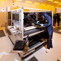
Among ISS’ key pieces of equipment is its £1.5 million ($2.4 million) Nilpeter press. The press can handle multiple printing techniques on paper, card, films and foil, producing thicknesses from 25 to 370 microns. ISS also offers a wide variety of printing, curing and cutting equipment. The ISS line can be utilized to produce prototypes, and can be scaled for pilot production.
“The facility has the capability to perform flexo, gravure, offset litho and rotary screen printing processes alongside cut/crease operations and pick and place technology,” said Alan McClelland, commercial business manager at CPI. “The line is open for commercial or grant-funded projects with the aim of producing demonstrator units and prototypes, as well as performing pilot production and scalable process development.”
McClelland added that the ISS facility is ideal for a wide range of users, including brand owners, printers, packaging houses, creative designers, ink formulators, substrate suppliers and equipment manufacturers.
The facility offers numerous advantages for companies and universities to test out new applications. ISS can print electronically interactive items such as point of sale material, toys, games, novelty items, smart packaging and intelligent sensors in a standard pressroom environment.
“Major markets for printed electronics include fast moving consumer goods (FMCG), pharmaceutical and retail, with new applications in smart, functional packaging, intelligent sensing and interactive point of sale materials that will be developed,” McClelland said. “In addition, the ability to create products with printed sensing will be of interest to the transport and construction markets.”
McClelland said that CPI’s expertise in design and development has allowed the group to carve out a successful niche in the PE marketplace.
“CPI’s focus is on design, development and prototyping for the emerging printable electronics industry,” McClelland noted. “Our role is to work with clients to bring new printable electronics products and processes to market quickly and efficiently, by offering the facilities and expertise that help reduce the level of R&D risk and capital investment, while speeding up time to market.”
“For organizations looking to prove and prototype their products and processes up to pre-production scale, CPI provides access to state-of-the-art printable electronics equipment and materials and provides support from industry experts to assist with applications in development and commercialization,” McClelland added.
McClelland noted that CPI also offers materials science knowledge that is proving helpful to the PE supply chain.
“CPI is developing a new range of organic semiconducting materials, which will be used to create the thin, flexible display screens of the future,” McClelland said. “There remain many challenges to introduction of some of these products, and CPI is working with universities, large corporations and SMEs; an example is CPI's ground-breaking work on barrier films to prevent moisture ingress and increase the lifespan of printed electronic components.”
McClelland said that CPI is supporting print, packaging and consumer goods companies now in the commercialization of interactive posters and smart packaging.
“These have the potential to engage consumers in the shop and at home,” McClelland added. “As conventional printing techniques can be used, these novel products could become familiar very soon. Conventional printing techniques may also speed the introduction of printed sensors for applications such as point-of-care medical diagnosis.”
The future is particularly exciting for the printed electronics field and CPI.
“In the coming years, we will see the leading edge equipment at CPI being used to support the development of printed, flexible solid state lighting and photovoltaics; and these thin, lightweight products could transform the space around us at home and in the car through innovative design,” McClelland concluded.
The Centre for Process Innovation (CPI) has had much success in this area. In April, CPI opened its Integrated Smart Systems (ISS) facility. CPI invested £2 million ($3.16 million) into its new facility, located at CPI’s National Printable Electronics Centre, NETPark, site at Sedgefield, UK.
The concept of CPI’s Integrated Smart Systems line was generated by The Northern Way Printed Electronics Technology Competition, a project to stimulate potential users of PE to explore near-to-market applications that could emerge from the technology. Following the opening of the facility, CPI’s ISS platform already has a list of projects running, including materials and ink suppliers, print and packaging houses, label converters, designers and automotive suppliers.
Among ISS’ key pieces of equipment is its £1.5 million ($2.4 million) Nilpeter press. The press can handle multiple printing techniques on paper, card, films and foil, producing thicknesses from 25 to 370 microns. ISS also offers a wide variety of printing, curing and cutting equipment. The ISS line can be utilized to produce prototypes, and can be scaled for pilot production.
“The facility has the capability to perform flexo, gravure, offset litho and rotary screen printing processes alongside cut/crease operations and pick and place technology,” said Alan McClelland, commercial business manager at CPI. “The line is open for commercial or grant-funded projects with the aim of producing demonstrator units and prototypes, as well as performing pilot production and scalable process development.”
McClelland added that the ISS facility is ideal for a wide range of users, including brand owners, printers, packaging houses, creative designers, ink formulators, substrate suppliers and equipment manufacturers.
The facility offers numerous advantages for companies and universities to test out new applications. ISS can print electronically interactive items such as point of sale material, toys, games, novelty items, smart packaging and intelligent sensors in a standard pressroom environment.
“Major markets for printed electronics include fast moving consumer goods (FMCG), pharmaceutical and retail, with new applications in smart, functional packaging, intelligent sensing and interactive point of sale materials that will be developed,” McClelland said. “In addition, the ability to create products with printed sensing will be of interest to the transport and construction markets.”
McClelland said that CPI’s expertise in design and development has allowed the group to carve out a successful niche in the PE marketplace.
“CPI’s focus is on design, development and prototyping for the emerging printable electronics industry,” McClelland noted. “Our role is to work with clients to bring new printable electronics products and processes to market quickly and efficiently, by offering the facilities and expertise that help reduce the level of R&D risk and capital investment, while speeding up time to market.”
“For organizations looking to prove and prototype their products and processes up to pre-production scale, CPI provides access to state-of-the-art printable electronics equipment and materials and provides support from industry experts to assist with applications in development and commercialization,” McClelland added.
McClelland noted that CPI also offers materials science knowledge that is proving helpful to the PE supply chain.
“CPI is developing a new range of organic semiconducting materials, which will be used to create the thin, flexible display screens of the future,” McClelland said. “There remain many challenges to introduction of some of these products, and CPI is working with universities, large corporations and SMEs; an example is CPI's ground-breaking work on barrier films to prevent moisture ingress and increase the lifespan of printed electronic components.”
McClelland said that CPI is supporting print, packaging and consumer goods companies now in the commercialization of interactive posters and smart packaging.
“These have the potential to engage consumers in the shop and at home,” McClelland added. “As conventional printing techniques can be used, these novel products could become familiar very soon. Conventional printing techniques may also speed the introduction of printed sensors for applications such as point-of-care medical diagnosis.”
The future is particularly exciting for the printed electronics field and CPI.
“In the coming years, we will see the leading edge equipment at CPI being used to support the development of printed, flexible solid state lighting and photovoltaics; and these thin, lightweight products could transform the space around us at home and in the car through innovative design,” McClelland concluded.