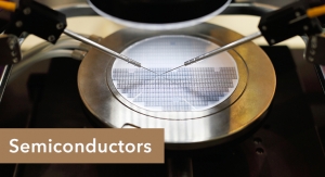
Printed Electronics Now Staff08.11.20
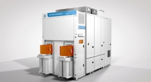
Applied Materials, Inc. announced a new addition to its successful Centris Sym3 etch product family, that now enables chipmakers to precisely pattern and shape ever-smaller features in leading-edge memory and logic chips.
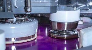
The new Centris Sym3® Y is Applied’s most advanced conductor etch system. It uses RF pulsing technology to provide the extremely high materials selectivity, depth control and profile control needed by customers to create densely packed, high-aspect-ratio structures in 3D NAND, DRAM and logic, including FinFETs and emerging gate-all-around architectures.
A unique technical feature of the Sym3 family is a high-conductance chamber architecture that provides exceptional etch profile control by quickly and efficiently exhausting the etch byproducts that can accumulate with each wafer pass. The Sym3 Y system extends the benefits of this successful architecture with a proprietary new coating material that protects critical chamber components, thereby further reducing defects and enhancing yields.
First introduced in 2015, the Sym3 etch system has become Applied’s fastest ramping product in company history, and the company has just shipped the 5,000th chamber.
The Sym3 family is key to Applied’s strategy of giving customers new ways to shape and pattern materials, enabling novel 3D structures and new ways to continue 2D shrinking.
“Applied took a clean-sheet approach to conductor etch with the Sym3 system launch in 2015 and solved some of the most difficult etch challenges in 3D NAND and DRAM,” said Dr. Mukund Srinivasan, VP and GM, Semiconductor Products Group at Applied Materials.