11.12.19
According to MarketandMarkets report "Electronic Chemicals and Materials Market by Type (Specialty Gases, CMP Slurries, Conductive Polymers, Photoresist Chemicals, Low K Dielectrics, Wet Chemicals, Silicon Wafers, PCB Laminates), Application, and Region - Global Forecast to 2024," the electronic chemicals and materials market size is estimated at $56.3 billion in 2019 and is projected to reach $81.6 billion by 2024, at a CAGR of 7.7% during the forecast period. Increasing demand from the microelectronics and chip manufacturing industries globally is expected to drive the market.
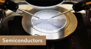
Silicon wafers are a thin slice of semiconductor, which is made out of crystalline silicon and is a key component in the fabrication of integrated circuits and serves as a substrate for the microelectronics devices. The primary use of silicon wafer is in integrated circuits, which are the basic building block of any electronic devices, such as computers and smartphones. Other applications include tire pressure systems and solar cells. The silicon wafers market is expected to grow in tandem with the growth of the integrated circuits and solar markets during the forecast period.
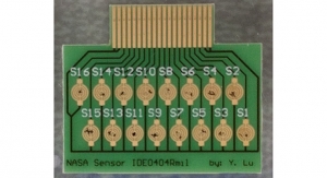
Any semiconductor device contains integrated circuits (ICs) and printed board circuit (PCB). ICs are an assembly of electronic components that are fabricated as a single unit, which includes actives devices and passive devices, such as transistors and capacitors along with their interconnections, which are built on a thin substrate of silicon material.
The final circuit formed is termed as chip. A printed circuit board is a circuit where all the components are contained within a mechanical structure. It is built by an alternating layer of conductive polymer along with layers of non-conductive insulation material.
APAC is the largest semiconductor market due to an increasing proportion of Chinese semiconductor products it’s the memory chip market in China, which generated most of the revenue of the semiconductor industry in the region.
Silicon wafers are a thin slice of semiconductor, which is made out of crystalline silicon and is a key component in the fabrication of integrated circuits and serves as a substrate for the microelectronics devices. The primary use of silicon wafer is in integrated circuits, which are the basic building block of any electronic devices, such as computers and smartphones. Other applications include tire pressure systems and solar cells. The silicon wafers market is expected to grow in tandem with the growth of the integrated circuits and solar markets during the forecast period.
Any semiconductor device contains integrated circuits (ICs) and printed board circuit (PCB). ICs are an assembly of electronic components that are fabricated as a single unit, which includes actives devices and passive devices, such as transistors and capacitors along with their interconnections, which are built on a thin substrate of silicon material.
The final circuit formed is termed as chip. A printed circuit board is a circuit where all the components are contained within a mechanical structure. It is built by an alternating layer of conductive polymer along with layers of non-conductive insulation material.
APAC is the largest semiconductor market due to an increasing proportion of Chinese semiconductor products it’s the memory chip market in China, which generated most of the revenue of the semiconductor industry in the region.