11.11.19
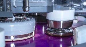
Applied Materials, Inc. announced the opening of the Materials Engineering Technology Accelerator (META Center), a first-of-its-kind facility aimed at speeding customer prototyping of new materials, process technologies and devices.
As chipmaking becomes increasingly challenging, the META Center extends Applied’s ability to collaborate with customers to pioneer new ways of improving chip performance, power and cost.
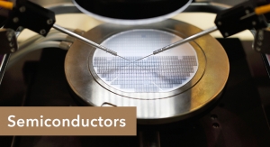
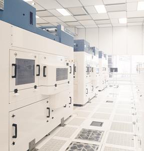
Located at the State University of New York Polytechnic Institute (SUNY Poly) campus in Albany, NY, the META Center’s cleanroom provides customers and partners access to state-of-the-art process systems to help shorten the time from lab to fab.
“We are excited to open the doors of the META Center and invite the industry to collaborate with us to accelerate innovation, from materials to systems,” said Steve Ghanayem, senior VP of New Markets and Alliances at Applied Materials.
“New York State is home to a thriving high-tech ecosystem and the opening of the META Center will keep us at the forefront of technology innovation,” Empire State Development Acting Commissioner and President & CEO-designate Eric Gertler said. “The partnership we’ve developed with NY CREATES, SUNY and Applied Materials will create the building blocks to bring new business, research, jobs and educational opportunities to the state for years to come.”
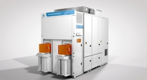
At the META Center, engineers can evaluate novel chip materials, structures and devices, testing them in a robust pilot manufacturing environment and accelerating their readiness for customer high-volume manufacturing facilities. Among the first chip devices under evaluation at the META Center is a new magnetic random-access memory (MRAM) targeted at Internet of Things devices, providing low-power, nonvolatile code storage and high-density working memory. Applied’s recently launched Endura CloverTM MRAM PVD platform is among the systems at the META Center enabling this capability.
The META Center is a strategic addition to Applied’s global R&D environment. It complements Applied’s Maydan Technology Center in Silicon Valley where new process systems are developed, along with the company’s Advanced Materials Lab and Advanced Packaging Development Center, both located in Singapore. Applied’s global R&D environment demonstrates the company’s commitment to a new playbook for industry innovation and collaboration, from materials to systems.
As chipmaking becomes increasingly challenging, the META Center extends Applied’s ability to collaborate with customers to pioneer new ways of improving chip performance, power and cost.
Located at the State University of New York Polytechnic Institute (SUNY Poly) campus in Albany, NY, the META Center’s cleanroom provides customers and partners access to state-of-the-art process systems to help shorten the time from lab to fab.
“We are excited to open the doors of the META Center and invite the industry to collaborate with us to accelerate innovation, from materials to systems,” said Steve Ghanayem, senior VP of New Markets and Alliances at Applied Materials.
“New York State is home to a thriving high-tech ecosystem and the opening of the META Center will keep us at the forefront of technology innovation,” Empire State Development Acting Commissioner and President & CEO-designate Eric Gertler said. “The partnership we’ve developed with NY CREATES, SUNY and Applied Materials will create the building blocks to bring new business, research, jobs and educational opportunities to the state for years to come.”
At the META Center, engineers can evaluate novel chip materials, structures and devices, testing them in a robust pilot manufacturing environment and accelerating their readiness for customer high-volume manufacturing facilities. Among the first chip devices under evaluation at the META Center is a new magnetic random-access memory (MRAM) targeted at Internet of Things devices, providing low-power, nonvolatile code storage and high-density working memory. Applied’s recently launched Endura CloverTM MRAM PVD platform is among the systems at the META Center enabling this capability.
The META Center is a strategic addition to Applied’s global R&D environment. It complements Applied’s Maydan Technology Center in Silicon Valley where new process systems are developed, along with the company’s Advanced Materials Lab and Advanced Packaging Development Center, both located in Singapore. Applied’s global R&D environment demonstrates the company’s commitment to a new playbook for industry innovation and collaboration, from materials to systems.