11.08.18
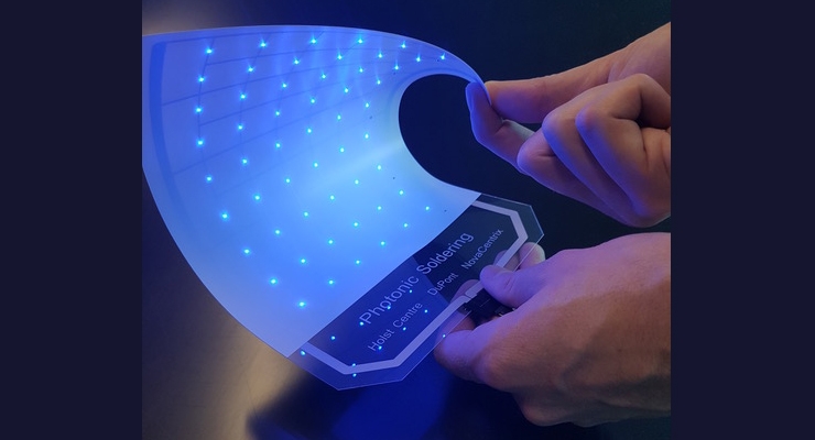
Photonic soldering, using PulseForge tools, is being developed in a partnership with Holst Centre (Eindhoven, Netherlands) and NovaCentrix (Austin, TX).
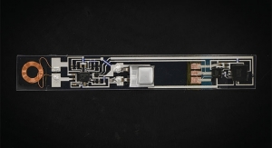
This new bonding technique attaches surface-mount electronics to low-melting point polymer films using standard lead-free solder in a matter of seconds.
Demand for high-performance multifunctional flexible systems is increasing. To deliver such systems, manufacturers need to be able to combine standard silicon ICs or surface mounted device (SMD) components with printed circuits on flexible plastic substrates. As chips get smaller, the density of interconnects gets higher, demanding higher-resolution interconnection technologies. Moreover, the low melting point of the plastics used in cost-effective substrates makes traditional thermal techniques impossible.
The team from Holst Centre and NovaCentrix have developed photonic soldering, a light-based technique that enables fast, high-resolution integration of silicon components onto flexible foils. Photonic soldering uses intense light pulses from advanced flash lamp systems to cure the solder paste within seconds. Only the solder paste is heated, not the substrate, thus making the technology compatible with low-cost films such as PET. The technique is compatible with roll-to-roll production for cost-effective high-volume production.
“Flexible hybrid systems require reliable interconnections between the printed and standard silicon components. Our light-assisted technique offers better mechanical stability and electrical connections than existing approaches, and is the only current means for using standard lead-free solder on low-melting-point plastic films,” said Francesca Chiappini, research scientist at Holst Centre.
“Using our state-of-the-art PulseForge tools, photonic soldering can cure off-the-shelf solder pastes on polymer films within 5 seconds. This is ideal for combining the performance and reliability of traditional electronics with the capabilities of flexible printed systems. As the newly-installed photonic soldering pilot line at Holst Centre shows, photonic soldering is ready for commercial-scale, high-throughput manufacturing,” added Stan Farnsworth, chief marketing officer at NovaCentrix.
Holst Centre researchers will be presenting the new technique, along with technology demonstrators and application prototypes, on Nov. 13, 2018, at SEMICON Europa in Munich, Germany. NovaCentrix will be presenting the technique and showing samples at Printed Electronics USA in Santa Clara, CA, Nov. 14-15 2018.