11.28.16
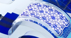
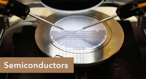
Fast and industry-compatible, spatial atomic layer deposition (sALD) may revolutionize production of thin-film displays. Researchers at Holst Centre have shown that sALD can deliver semiconductor layers with better performance than physical vapor deposition (PVD) at the same – and potentially even higher – throughputs. An easily scalable, atmospheric-pressure process, sALD could soon become the preferred method for creating large-area thin-film and flexible devices.
A key step in producing next-generation ultra-high definition displays is the creation of a highly uniform layer of an amorphous oxide semiconductor such as indium-gallium zinc oxide (IGZO). Today, this is typically done using a PVD technique known as sputter deposition. Sputtering requires expensive vacuum equipment and can also prove difficult to correctly control material composition and thickness over large areas. This results in variable transistor performance, particularly in thin film applications such as displays.
Now Holst Centre has shown that sALD offers an industry-compatible alternative which improves display performance and at the same time could cut production costs. The team has used the technique to create semiconductor layers with charge carrier mobilities (a key measure of semiconductor performance) of 30 to 45 cm2/Vs. This compares to typical mobilities around 10 cm2/Vs for sputtering.
“The performance of sALD means semiconductor layers could become much thinner, enabling even higher throughputs and lower material consumption,” added Gerwin Gelinck, program director flexible and large area transistor electronics at Holst Centre. “In fact, its performance characteristics are preserved even when scaling down the semiconductor thickness to less than 5 nm. This can lead to novel semiconductor structures, such as super-lattices, with even higher electron mobilities.”
The Holst Centre team and partners are now taking steps towards the upscaling and commercialization of these sALD processes and related equipment.