04.15.16
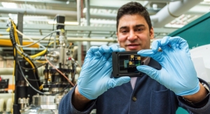
Imec and Crystal Solar announced that they have achieved a 22.5% cell efficiency (certified by FhG ISE CalLab) with nPERT silicon (Si) solar cells manufactured on 6-inch mono-crystalline epitaxially grown kerfless wafers. Marking an industry first, imec and Crystal Solar have demonstrated the highest efficiency to-date for homojunction solar cells on epitaxially grown silicon wafers, paving the way toward industrialization of this promising technology.
Crystal Solar’s breakthrough manufacturing technology called Direct Gas to Wafer enables direct conversion of feedstock gas to mono crystalline silicon wafers by high throughput epitaxial growth. By skipping the polysilicon, ingoting and the wire-sawing steps altogether, this approach not only results in lowest cost/watt for the wafers but also significantly reduces the capital required to set up a manufacturing plant.
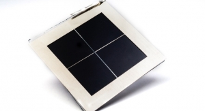
Imec has adapted its highly efficient nPERT Si solar cell process to align with the properties of Crystal Solar’s kerfless wafers. The 156x156mm2 cells were fabricated on 160 to 180 um thick grown n-type wafers with built-in rear p+ emitter. Imec’s n-PERT process included a selective front surface field realized by laser doping, advanced emitter surface passivation by Al2O3 and Ni/Cu plated contacts.
The novel process using all industrially available processing steps resulted in record efficiencies for homojunction large area solar cells of 22.5% and a record Voc of 700mV. This high Voc illustrates the high quality of the wafers and the built-in junction.
“This approach represents a new paradigm in cell manufacturing with its unique ability to bypass significant steps in both wafer and cell manufacturing thereby dramatically reducing the capex and the overall cost per watt,” said T.S. Ravi, CEO of Crystal Solar. “We expect to achieve >23% efficiencies with imec’s PERT technology in the very near future.”
Crystal Solar’s breakthrough manufacturing technology called Direct Gas to Wafer enables direct conversion of feedstock gas to mono crystalline silicon wafers by high throughput epitaxial growth. By skipping the polysilicon, ingoting and the wire-sawing steps altogether, this approach not only results in lowest cost/watt for the wafers but also significantly reduces the capital required to set up a manufacturing plant.
Imec has adapted its highly efficient nPERT Si solar cell process to align with the properties of Crystal Solar’s kerfless wafers. The 156x156mm2 cells were fabricated on 160 to 180 um thick grown n-type wafers with built-in rear p+ emitter. Imec’s n-PERT process included a selective front surface field realized by laser doping, advanced emitter surface passivation by Al2O3 and Ni/Cu plated contacts.
The novel process using all industrially available processing steps resulted in record efficiencies for homojunction large area solar cells of 22.5% and a record Voc of 700mV. This high Voc illustrates the high quality of the wafers and the built-in junction.
“This approach represents a new paradigm in cell manufacturing with its unique ability to bypass significant steps in both wafer and cell manufacturing thereby dramatically reducing the capex and the overall cost per watt,” said T.S. Ravi, CEO of Crystal Solar. “We expect to achieve >23% efficiencies with imec’s PERT technology in the very near future.”