11.19.15
Nano Dimension Ltd. showed the world’s first desktop-sized 3D printer designed specifically for the production of professional multilayer printed circuit boards (PCBs). The DragonFly 2020 3D Printer, demonstrated in the US for the first time at the Printed Electronics USA 2015 conference, will allow users to build functional, multilayer circuit board prototypes in-house in a matter of hours.
The capability of rapidly producing functional multilayer PCB prototypes using 3D printing is new to the printed electronics design and manufacturing industry. The current standard subtractive manufacturing of PCBs is a multi-stage, labor- and material-intensive process, and is so costly and time consuming that electronics designers requiring prototypes resort to outsourcing.
Nano Dimension’s 3D printer can print a complete multilayer PCB, including all interconnections between layers, using its revolutionary inkjet printer and highly conductive nano inks.
“For designers and engineers looking for ultra-rapid prototyping of PCBs, our 3D printer is a significant leap forward,” said Simon Fried, chief marketing officer at Nano Dimension. “Moving their work from design to a prototype at an off-site printing facility might take weeks for the PCB to be ordered, produced and shipped. If further iterations are needed, it’s back to the prototyping house for another cycle.
“In today’s competitive electronics markets, unforeseeable and costly delays during PCB development can significantly slow time-to-market,” Fried added. “That’s the development risk and bottleneck that we’re eliminating with the DragonFly 2020.”
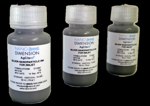
Nano Dimension also exhibited its AgCite line of conductive silver nanoparticle inks for inkjet deposition and 3D printed PCB prototype samples.
The DragonFly 2020 3D Printer is targeted for commercial availability during the second half of 2016. The AgCite conductive inks are available today.
The capability of rapidly producing functional multilayer PCB prototypes using 3D printing is new to the printed electronics design and manufacturing industry. The current standard subtractive manufacturing of PCBs is a multi-stage, labor- and material-intensive process, and is so costly and time consuming that electronics designers requiring prototypes resort to outsourcing.
Nano Dimension’s 3D printer can print a complete multilayer PCB, including all interconnections between layers, using its revolutionary inkjet printer and highly conductive nano inks.
“For designers and engineers looking for ultra-rapid prototyping of PCBs, our 3D printer is a significant leap forward,” said Simon Fried, chief marketing officer at Nano Dimension. “Moving their work from design to a prototype at an off-site printing facility might take weeks for the PCB to be ordered, produced and shipped. If further iterations are needed, it’s back to the prototyping house for another cycle.
“In today’s competitive electronics markets, unforeseeable and costly delays during PCB development can significantly slow time-to-market,” Fried added. “That’s the development risk and bottleneck that we’re eliminating with the DragonFly 2020.”
Nano Dimension also exhibited its AgCite line of conductive silver nanoparticle inks for inkjet deposition and 3D printed PCB prototype samples.
The DragonFly 2020 3D Printer is targeted for commercial availability during the second half of 2016. The AgCite conductive inks are available today.